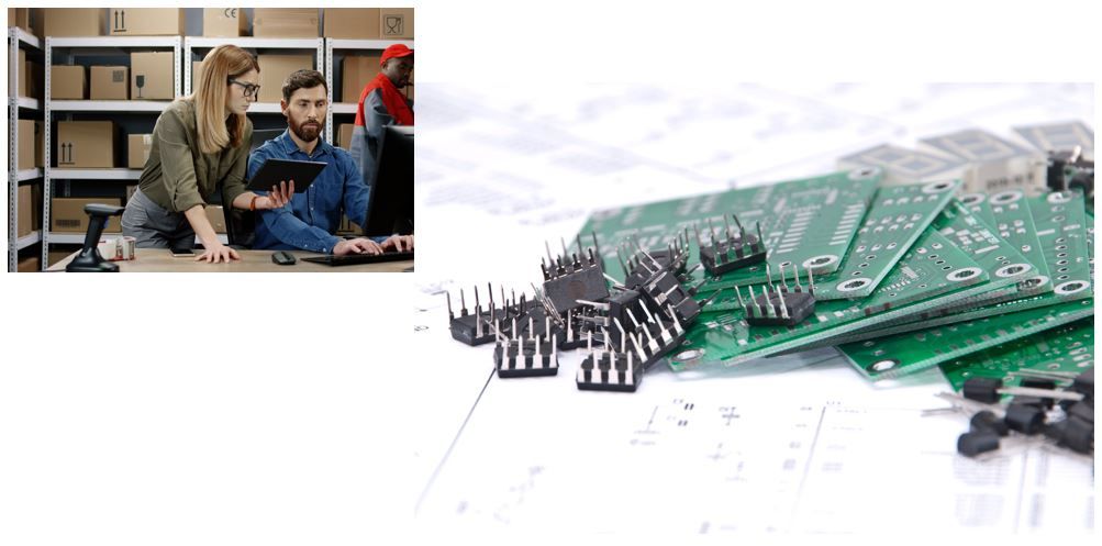
Official definition of a Kit is “a set of materials or parts from which something can be assembled…” and the definition of Kitting is “to package or make available in a kit”. Kitting has been the primary focus of the Project Coordinators at California Integration Coordinators, Inc. since 1988. With our depth of experience, it is our privilege to explain what Kitting means for the PCB assembly.
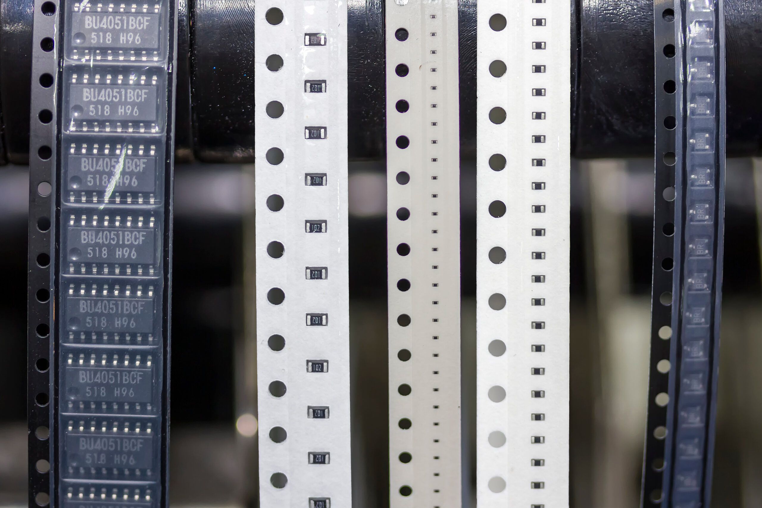
The Bill of Materials (BoM) is the starting point for the PCB Kit. The Project Coordinators quote every requirement on the BoM with pricing, lead-time, and MOQ (minimum order quantity). The quote will also include any life-cycle alert, and an engineer vetted suggested alternate, if the lead-time is outside the project scope, or if the call-out is obsolete. If the build quantity is low volume, the Project Coordinator will maximize project funds by quoting broken packaging options such as cut tape rather than full reel quantities. Further cost savings can be utilized by minimizing attrition on expensive components and adding leader / trailer to the materials.
The true value of the Project Coordinators managing the procurement and kitting, is in their understanding of all assembly elements that drive high yields and successful PCB placements. Elements such as assembly attrition specifications, component verification, packaging options, as well as the documentation requirements and continuous status updates.
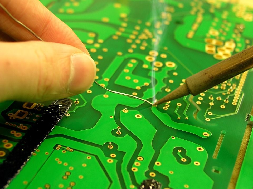
Completed Kits for PCB Assembly arrive at the assembly facility in BoM Line-Item order, with the documentation package, for ease of the assembly audit process. The Kit has the attrition needed to provide for a successful full-yield assembly.
If further questions arise on Kitting for PCB assembly, please feel free to reach out to us at www.cic-inc.com or email us at cic@cic-inc.com.